Connect with us

Technology

Scanning Electron Microscope (SEM) Market to Grow by USD 1.08 Billion from 2024-2028, Driven by Focus on Nanotechnology and AI’s Role in Market Transformation – Technavio

Published

on

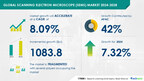
NEW YORK, Oct. 1, 2024 /PRNewswire/ — Report on how AI is driving market transformation – The Global Scanning Electron Microscope (SEMS) Market size is estimated to grow by USD 1.08 billion from 2024-2028, according to Technavio. The market is estimated to grow at a CAGR of over 8.09% during the forecast period. Increasing focus on nanotechnology is driving market growth, with a trend towards increased demand for LVEMS. However, high cost of scanning electron microscope poses a challenge – Key market players include Advantest Corp., Agilent Technologies Inc., Bruker Corp., Carl Zeiss Stiftung, COXEM Co. Ltd., Danaher Corp., DELONG INSTRUMENTS AS, Hirox Co. Ltd., Hitachi Ltd., HOVERLABS, JEOL Ltd., Keysight Technologies Inc., Nikon Corp., Nion, Olympus Corp., Seiko Holdings Corp., TESCAN GROUP, Thermo Fisher Scientific Inc., Tokyo Instruments Inc., and Topcon Corp..

Key insights into market evolution with AI-powered analysis. Explore trends, segmentation, and growth drivers- View the snapshot of this report

Scanning Electron Microscope (SEMS) Market Scope

Report Coverage

Details

Base year

2023

Historic period

2018 – 2022

Forecast period

2024-2028

Growth momentum & CAGR

Accelerate at a CAGR of 8.09%

Market growth 2024-2028

USD 1083.8 million

Market structure

Fragmented

YoY growth 2022-2023 (%)

7.32

Regional analysis

APAC, North America, Europe, South America, and Middle East and Africa

Performing market contribution

APAC at 42%

Key countries

US, China, Japan, Germany, and South Korea

Key companies profiled

Advantest Corp., Agilent Technologies Inc., Bruker Corp., Carl Zeiss Stiftung, COXEM Co. Ltd., Danaher Corp., DELONG INSTRUMENTS AS, Hirox Co. Ltd., Hitachi Ltd., HOVERLABS, JEOL Ltd., Keysight Technologies Inc., Nikon Corp., Nion, Olympus Corp., Seiko Holdings Corp., TESCAN GROUP, Thermo Fisher Scientific Inc., Tokyo Instruments Inc., and Topcon Corp.


Market Driver

Scanning electron microscopes (SEMs) come in two main varieties: high-voltage electron microscopes (HVEMs) and low-voltage electron microscopes (LVEMs). While HVEMs operate at a high voltage of 100 kilovolts, LVEMs function at a reduced voltage of less than 25 kilovolts. This difference makes LVEMs more compact and cost-effective, allowing them to be used as tabletop or desktop microscopes. LVEMs are particularly suitable for specimens with a low atomic number, such as polymers, composite materials, pigments, minerals, cells, and membranes. These microscopes cause minimal damage to specimens due to lower radiation and offer high contrast. In contrast, HVEMs can damage specimens due to high radiation accumulation. LVEMs have gained popularity in life science, material science, pathology, and nanomaterial applications. Delong America is a leading vendor in this segment, offering products like LVEM5 and LVEM25, which function as both TEM and SEM. Although LVEMs are priced lower than conventional electron microscopes, they do not match their magnification capabilities. The increasing demand for LVEMs in various industries is expected to fuel the growth of the global scanning electron microscope market. 

The Scanning Electron Microscope (SEM) market is experiencing significant growth due to increasing trends in nanotechnology and electronics. With the miniaturization of transistor chips and the demand for high resolution nanoscale imaging, SEMs play a crucial role in surface morphology analysis and chemical composition identification. The market caters to various industries including electronics, life sciences, and material sciences. Nanotechnology applications in areas like nanofibers, nanotubes, temperature superconductors, and alloy strength are driving the demand for SEMs. However, high excise taxes and custom duties pose challenges for market expansion. SEMs are used for failure analysis, drug development, material characterization, and correlative microscopy techniques like light microscopy and atomic force microscopy. Industries like aerospace, defense, and medical devices also rely on SEMs for quality control and clinical trials. Advancements in detector technology and the introduction of compact, high vacuum, low vacuum, cryo-SEM, environmental SEM, field emission SEM, tabletop SEM, dual-beam SEM, and other models continue to boost market growth. 

Request Sample of our comprehensive report now to stay ahead in the AI-driven market evolution!

 Market Challenges

The Scanning Electron Microscope (SEM) market is currently experiencing a challenge due to the high cost of SEMs, which is limiting demand. SEMs range in price from USD100,000 to USD1,250,000, with non-analytical models costing approximately USD700,000. Most vendors sell SEMs in this price range, while analytical models cost between USD400,000 and USD620,000. The price depends on the model’s specifications and accessories. Organizations face budget constraints, making it difficult to purchase SEMs. Educational institutions and research organizations, which are significant buyers, depend on external funding, leading to uncertain sales. The high cost also impacts overseas sales due to customs taxes, which can reach up to 30% of the product cost. Potential customers often opt for renting SEMs instead, affecting new product sales. The price difference between new and used SEMs can be significant, reaching up to 50% or more. Consequently, the high cost of SEMs is expected to restrict market growth during the forecast period.The Scanning Electron Microscope (SEM) market is experiencing significant growth due to its applications in various industries. Nanotechnology is a key driver, with SEMs used to examine nanofibers, nanotubes, and other nanoscale structures in materials science and biology. Chronic diseases and drug development also benefit from SEMs’ high-resolution imaging capabilities. In industries like aerospace, defense, and environmental science, SEMs are used for material characterization and failure analysis. SEMs are also essential in research institutions for studying temperature superconductors, alloy strength, and other advanced materials. With the increasing demand for user-friendly software, compact models, and correlative microscopy techniques, SEMs are becoming more accessible to a wider range of users. New technologies like Cryo-SEM, Low vacuum SEM, and Field emission SEM are expanding the applications of SEMs, while automated features and intelligent technology enhance their efficiency. SEMs are also used in forensics and semiconductor manufacturing for specimen analysis and high-energy beam applications. Overall, the SEM market is poised for continued growth in various industries due to its versatility and importance in material science, nanotechnology, and research and development.

Discover how AI is revolutionizing market trends- Get your access now!

Segment Overview 

This scanning electron microscope (sems) market report extensively covers market segmentation by

Type 1.1 Tabletop1.2 ConventionalEnd-user 2.1 Semiconductor2.2 Life sciences2.3 Material sciences2.4 NanotechnologyGeography 3.1 APAC3.2 North America3.3 Europe3.4 South America3.5 Middle East and Africa

1.1 Tabletop- The tabletop segment of the global scanning electron microscope (SEM) market refers to compact and portable SEM systems designed for easy installation and use in laboratories and educational institutions. Their smaller size and affordability make tabletop SEMs an accessible and cost-effective option for researchers and educators in small facilities. These systems offer high-resolution imaging capabilities with efficient data acquisition, enabling quick analysis and increased productivity. Tabletop SEMs cater to various applications in materials science, nanotechnology, life sciences, and more, expanding their value to researchers and institutions. With user-friendly interfaces and simplified operations, these systems are suitable for users of all experience levels. Their maintenance requirements are also less complex compared to larger SEM systems, reducing operational downtime and costs. These factors are expected to fuel the growth of the tabletop segment in the global SEM market.

Download a Sample of our comprehensive report today to discover how AI-driven innovations are reshaping competitive dynamics

Research Analysis

The Scanning Electron Microscope (SEM) market encompasses nanotechnology applications in various industries, including the semiconductor industry, electronics, and materials science. SEMs utilize electron beams to achieve high-resolution imaging at the nanoscale, revealing surface morphology, chemical analysis, fractography, and other critical details. These microscopes are essential for nanoscale imaging and analysis in sectors such as nanotechnology, nanoscale materials, and medical research. SEMs offer magnification capabilities far beyond light microscopy, enabling the examination of high-energy beam-sensitive specimens and nanoscale structures. They are indispensable tools for semiconductor wafer analysis, materials science, and biology. Correlative microscopy techniques, such as SEM-Atomic Force Microscopy (AFM), further expand their capabilities. Detector technology advancements continue to improve resolution power, making SEMs an intelligent technology for high-precision analysis and research.

Market Research Overview

The Scanning Electron Microscope (SEM) market encompasses various industries, including nanotechnology, electronics, life sciences, material sciences, and more. SEMs utilize electron beams to achieve high-resolution imaging of nanoscale structures, providing valuable information on surface morphology, chemical analysis, fractography, and more. Applications span from nanofibers and nanotubes in material sciences to temperature superconductors and alloy strength in aerospace and defense. SEMs are essential for miniaturization in electronics, such as transistor chips, and for quality control in manufacturing processes. Sample preparation is a critical aspect of SEM analysis, with various techniques employed to ensure accurate results. High excise taxes and custom duties pose challenges to the market, particularly for research institutions and smaller businesses. Advanced detector technology, user-friendly software, and automated features are driving the development of compact SEMs and other innovative SEM models, including high vacuum, low vacuum, cryo-SEM, environmental SEM, field emission SEM, tabletop SEM, dual-beam SEM, and more. SEMs play a crucial role in failure analysis, drug development, material characterization, and various fields, including biology, correlative microscopy techniques, and forensics. Intelligent technology and automated features are enhancing the capabilities of SEMs, enabling new applications in nanotechnology, medical research, and semiconductor wafers. High-energy beam magnification and specimen analysis are key features that enable SEMs to provide valuable insights into nanoscale materials and structures.

Table of Contents:

1 Executive Summary
2 Market Landscape
3 Market Sizing
4 Historic Market Size
5 Five Forces Analysis
6 Market Segmentation

TypeTabletopConventionalEnd-userSemiconductorLife SciencesMaterial SciencesNanotechnologyGeographyAPACNorth AmericaEuropeSouth AmericaMiddle East And Africa

7 Customer Landscape
8 Geographic Landscape
9 Drivers, Challenges, and Trends
10 Company Landscape
11 Company Analysis
12 Appendix

About Technavio

Technavio is a leading global technology research and advisory company. Their research and analysis focuses on emerging market trends and provides actionable insights to help businesses identify market opportunities and develop effective strategies to optimize their market positions.

With over 500 specialized analysts, Technavio’s report library consists of more than 17,000 reports and counting, covering 800 technologies, spanning across 50 countries. Their client base consists of enterprises of all sizes, including more than 100 Fortune 500 companies. This growing client base relies on Technavio’s comprehensive coverage, extensive research, and actionable market insights to identify opportunities in existing and potential markets and assess their competitive positions within changing market scenarios.

Contacts

Technavio Research
Jesse Maida
Media & Marketing Executive
US: +1 844 364 1100
UK: +44 203 893 3200
Email: media@technavio.com
Website: www.technavio.com/

View original content to download multimedia:https://www.prnewswire.com/news-releases/scanning-electron-microscope-sem-market-to-grow-by-usd-1-08-billion-from-2024-2028–driven-by-focus-on-nanotechnology-and-ais-role-in-market-transformation—technavio-302264288.html

SOURCE Technavio

Continue Reading
Click to comment

Leave a Reply

Your email address will not be published. Required fields are marked *

Technology

Oracle to Invest More Than US$6.5 Billion in AI and Cloud Computing in Malaysia

Published

on

By

Oracle plans to open a cloud region in Malaysia, including 150+ infrastructure and SaaS services, to help boost the country’s digital economy and drive AI-fueled innovation  

Organizations across Malaysia can accelerate AI innovation with Oracle Cloud Infrastructure’s high performance and built-in security, powerful data, and distributed cloud capabilities

Upcoming cloud region to extend OCI’s footprint in Asia Pacific to 12 public cloud regions

AUSTIN, Texas and KUALA LUMPUR, Malaysia, Oct. 2, 2024 /PRNewswire/ — To meet the rapidly growing demand for its artificial intelligence (AI) and cloud services in Malaysia, Oracle today announced plans to invest more than US$6.5 billion to open a public cloud region in the country. The upcoming cloud region will enable Oracle customers and partners in Malaysia to leverage AI infrastructure and services and migrate mission-critical workloads to Oracle Cloud Infrastructure (OCI).

The planned public cloud region will help organizations in Malaysia modernize their applications, migrate all types of workloads to the cloud, and innovate with data, analytics, and AI. Customers can have access to OCI Generative AI Agents with retrieval-augmented generation (RAG) capabilities; accelerated computing and generative AI services to help keep sovereign AI models within country borders; and OCI Supercluster, the largest AI supercomputer in the cloud—orderable with up to 131,072 NVIDIA Blackwell GPUs with NVIDIA ConnectX-7 NICs for RoCEv2 networking or NVIDIA GB200 NVL72 rack solutions using liquid cooling and NVIDIA Quantum-2 InfiniBand networking. In addition, 150+ services, including Oracle Autonomous DatabaseHeatWave MySQL Database ServiceOracle Cloud VMware Solution, OCI Kubernetes Engine, and Oracle Fusion Cloud Applications Suite will also be available, offering customers infrastructure, platform, or SaaS services.

“We warmly welcome Oracle’s US$6.5 billion investment in Malaysia, which represents yet another expansion of their 36-year footprint in Malaysia,” said YB Senator Tengku Datuk Seri Utama Zafrul Tengku Abdul Aziz, minister of investment, trade and industry (MITI), Malaysia. “This investment will empower Malaysian entities, especially small and medium-sized enterprises, with innovative and cutting-edge AI and cloud technologies to enhance their global competitiveness. It is also a significant step towards realising the country’s New Industrial Master Plan’s ambitious vision of creating 3,000 smart factories by 2030. Oracle’s decision to establish a public cloud region in Malaysia underscores Malaysia’s infrastructure readiness, and its growing position as a premier Southeast Asian destination for digital investments.” 

Malaysia offers unique growth opportunities for organizations looking to accelerate their expansion with the latest digital technologies,” said Garrett Ilg, executive vice president and general manager, Japan & Asia Pacific, Oracle. “Our multi-billion dollar investment affirms our commitment to Malaysia as a regional gateway for cloud infrastructure as well as a comprehensive suite of SaaS applications deployed within Malaysia.”

“Rapidly growing demand for AI services prompts calls for more data centers that store large amounts of data and computational power to train and deploy AI models,” said Franco Chiam, vice president, cloud, data center and future digital infrastructure, Asia Pacific, IDC. “According to IDC FutureScape ‘The Infrastructure and Cloud Impact 2024 Predictions’, Malaysia’s public cloud services market is expected to grow by 27.2 percent CAGR from 2022 to 2027. The upcoming Oracle cloud region in Malaysia, therefore, signals the country’s potential to become a hub for technological innovation and growth in Southeast Asia.”

OCI Provides Customers with the Latest AI Infrastructure Offerings and a Resilient and Scalable Cloud Foundation Running Within Malaysia’s Borders

Oracle is the only hyperscaler capable of delivering AI and a full suite of 150+ cloud services across public, dedicated, and hybrid cloud environments, anywhere in the world. OCI’s unique cloud architecture enables Oracle to launch more public cloud regions faster by starting with an optimal footprint and scaling as needed, and deploy dedicated cloud regions with hyperscale cloud services inside customer data centers. This approach helps meet the needs of all countries and markets without compromising cloud capabilities, while also providing the consistent performance, SLAs, and global pricing for which OCI has become known.

With the planned public cloud region in Malaysia, customers and partners can gain low-latency access to cloud services to help them derive better value from their data and securely store data and run applications to help address regulations and requirements for data residency within Malaysia. In addition, OCI’s sovereign AI capabilities provide customers with increased control over where they locate their data and computing infrastructure and how they manage it. As a result, customers can achieve AI sovereignty by gaining the assurance that their use of AI is aligned with digital sovereignty frameworks.

Customers in Malaysia Welcome the Upcoming Public Cloud Region

Several NVIDIA AI infrastructure services will be available to customers, including NVIDIA AI Enterprise, NVIDIA Omniverse, and NVIDIA DGX Cloud.

“NVIDIA underpins the world’s largest AI models for training and inferencing, and Oracle’s continued expansion in Malaysia will help organizations across the country harness the power of AI,” said Dennis Ang, senior director, enterprise business (ASEAN and ANZ region), NVIDIA. “With the new Oracle Cloud Malaysia Region, customers in Malaysia will gain local access to NVIDIA’s accelerated, secure, and scalable platform for end-to-end AI development and deployment on OCI, helping accelerate the development of generative AI applications.”

Read the full release here.


View original content:https://www.prnewswire.com/apac/news-releases/oracle-to-invest-more-than-us6-5-billion-in-ai-and-cloud-computing-in-malaysia-302264649.html

SOURCE Oracle

Continue Reading

Technology

Farasis Energy Signs Strategic Agreement for Solid-State Batteries with JMEV; First SPS Battery for JMEV’s ‘ELIGHT’ Model Rolls Off the Production Line

Published

on

By

GANZHOU, China, Oct. 1, 2024 /PRNewswire/ — On September 29, JMEV and Farasis Energy signed a strategic cooperation agreement for the development of solid-state batteries, with the SPS (Super Pouch Solution) battery for the ‘ELIGHT’ model rolling off the production line at the same time.

According to the agreement, both parties aim to jointly promote the research, production, and market application of solid-state batteries. This includes accelerating the research and development of key technologies for solid-state batteries, facilitating industrial transformation and upgrading, and advancing the maturity and commercialization process of solid-state battery technology.

Solid-state batteries are seen as a competitive edge in new energy vehicle technology due to their high energy density, fast charging, long cycle life, and enhanced safety. Farasis Energy has been deeply engaged in areas such as electrochemical systems and Pouch batteries stacking processes for many years, perfectly aligning with the development path of solid-state batteries. The product development strategy focuses on medium- to long-term R&D goals for solid-state batteries that are high-energy, high-rate, high-safety, and low-cost, ensuring timely conversion of research achievements.

Currently, Farasis Energy’s first-generation semi-solid batteries have been mass-produced for passenger vehicles and have made breakthroughs in the commercial vehicle sector, forming a strategic alliance with FAW Jiefang to jointly promote the market and industrial chain development of semi-solid and solid-state batteries for commercial vehicles. Farasis Energy aims to complete the transition from semi-solid to solid-state battery commercialization within the next five years.

On the same day, the first SPS battery system of from Farasis Energy, designed to support the “ELIGHT” model, came off the production line. This follows previous supplies to Geely Radar Horizon and GAC Second-Gen Aion V models. The launch of the “ELIGHT” model’s SPS battery aims to assist JMEV in upgrading its pure electric platform and creating a pioneering sports sedan for a better travel experience.

Farasis Energy’s SPS features:

A 10-minute charge for a 400-kilometer rangeApplicability to chassis heights from 85mm to 145mmA volume utilization rate of up to 75%Full chemical system compatibility, including sodium ion batteries, lithium iron phosphate, and semi-solid batteries, etc.


View original content to download multimedia:https://www.prnewswire.com/news-releases/farasis-energy-signs-strategic-agreement-for-solid-state-batteries-with-jmev-first-sps-battery-for-jmevs-elight-model-rolls-off-the-production-line-302264911.html

SOURCE Farasis Energy

Continue Reading

Technology

Matterport Fall 2024 Release: Insights Meets Imagination elevates the platform with generative AI and more

Published

on

By

Matterport introduces essential new tools for real estate agents, contractors and designers

SINGAPORE, Oct. 2, 2024 /PRNewswire/ — Matterport, Inc., today unveiled a groundbreaking suite of new tools designed to reshape the way professionals design, build, and market properties.

Through the power of generative AI, Matterport users can now easily reimagine the potential of any space, transforming digital twins from static replicas into dynamic canvases for creativity.

“Our Fall 2024 Release empowers users to unlock the full potential of Matterport,” said RJ Pittman, Chairman and CEO of Matterport. “Imagine being able to defurnish a home with one click or generate stunning property descriptions automatically, using just the data from your digital twin. These tools save time, elevate listings, and simplify complex workflows for everyone—from real estate agents to contractors and enterprise teams. And with features like 3D model merge, field tags, and one-click bill-back processing, we’re helping customers manage spaces at scale with unprecedented speed, efficiency and precision.”

New tools for agents:

One of the most revolutionary additions in the Fall Release is Matterport’s AI-powered defurnish tool, designed to solve a common challenge for home sellers and agents: clutter. With a single click, users can now transform a cluttered living room or messy garage into a clean, open space—allowing potential buyers to visualize the home’s true potential. Whether it’s “erasing” an outdated couch or clearing out the dining room set, defurnish gives agents a powerful yet simple tool to make every property shine.

And coming soon, Matterport’s interior design tools will unlock creativity for everyone—letting users digitally furnish and redesign spaces with ease and offering a glimpse of what the future could hold.

The AI-powered property description tool is another game-changer, crafting detailed, engaging written descriptions in just seconds. Brokers and marketers can select the style and tone, ensuring each listing is perfectly tailored—whether it’s a sleek, modern downtown loft or a charming suburban home. And by leveraging the precise spatial data of every digital twin, the tool creates content that is not only beautifully written but also accurate down to the last detail, saving hours of work and producing results that even seasoned experts will admire.

New tools for property managers, contractors, and designers:

For large-scale projects, Matterport’s new Merge tool enables users to seamlessly “snap” together multiple digital twins. Imagine creating a full digital model of an entire hotel, floor by floor, or merging every floor of a high-rise office tower into one cohesive 3D tour of the building. Merge also allows multiple team members to scan different sections of a property simultaneously and integrate them later, making it possible to capture and manage even the most expansive buildings quickly and efficiently.

Field Tags further enhance the efficiency of on-site work by allowing users to add on-site observations and tags during the scanning process. No more repeat visits to capture missed details—everything can be documented in real-time, ensuring accurate, comprehensive records of the space are captured at the moment they matter most. This feature keeps teams aligned and projects moving forward without unnecessary delays.

Lastly, Matterport introduces one-click bill-back processing, a highly anticipated feature for enterprise customers. This simple yet powerful tool removes the headache of manual invoicing and cost allocation, allowing organizations to easily distribute expenses across departments and external partners. By automating billing processes, Matterport reduces administrative burdens and empowers teams to focus on what matters most.

About Matterport

Matterport, Inc. (Nasdaq: MTTR) is the World’s #1 Digital Twin Platform* leading the digital transformation of the built world. Our groundbreaking platform turns buildings into data to make every space more valuable and accessible. Millions of buildings in more than 177 countries have been transformed into immersive Matterport digital twins to improve every part of the building lifecycle from planning, construction, and operations to documentation, appraisal, and marketing. Learn more at matterport.com and browse a gallery of digital twins.

For additional information on the press release, promotions and updates, please follow Matterport on Twitter, Facebook , Linkedin  and Youtube page. Also, reach us for a complimentary demo or email cs-webinars@matterport.com for any related inquiries.

View original content to download multimedia:https://www.prnewswire.com/apac/news-releases/matterport-fall-2024-release-insights-meets-imagination-elevates-the-platform-with-generative-ai-and-more-302263322.html

SOURCE Matterport Pte Ltd

Continue Reading

Trending