The 2025 CES in the United States is about to unveil a brand-new chapter in the future intelligent home gardening
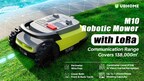
LAS VEGAS, Dec. 28, 2024 /PRNewswire/ — UBHOME, a sub-brand of UBTECH Robotics, announced an intelligent service robot in collaboration with Qualcomm Technologies, Inc. The Robotic Mower M10 is a revolutionary smart lawn mower announced at the 2025 International Consumer Electronics Show (CES) in the United States. This product is powered by the Qualcomm® RB1 Robotics Platform, showcases UBHOME’s rich experience in robot research and development, and focuses on solving the pain points of traditional lawn-mowing equipment, providing users with a worry-free and labor-saving smart gardening experience, and creates a new model of gardening intelligence.
User-Oriented: The All-New Convenience Brought by the Smart Lawn Mower to Life
The Robotic Mower M10 is not only a high performance tool but also an upgrade of the smart lifestyle. In response to the pain points of users when using traditional lawn-mowing equipment, this product offers a series of practical functions, bringing brand-new convenience to home gardening:
Wireless and Borderless Mowing: There is no need for cumbersome boundary wire installation anymore. The device relies on accurate environmental perception and navigation technology to independently plan the work area, allowing users to use it right out of the box, saving installation time and energy.
Automatic Mowing, Saving Time and Effort: The device can automatically complete the lawn mowing work according to the preset schedule or real-time instructions, enabling users to manage the lawn care through delegation to the mower.
Wide Coverage and Stable Signal: It supports a large-scale signal connection of up to 130,000 square meters. Even for extremely large courtyards, stable operation can be ensured, and there is no need to worry about signal loss.
Real-time Online, in-control Anytime: Through APP remote control and real-time monitoring, users can adjust the mowing plan or check the device status at any time, managing the courtyard work as they like.
The combination of these functions not only greatly simplifies the complexity of mowing work but also liberates users from repetitive physical labor, allowing them to focus on enjoying the wonderful moments of life.
UBHOME: In-depth Layout in Smart Home
UBHOME is a brand under UBTECH Robotics that focuses on providing smart solutions for families. As a world-leading robot enterprise, UBTECH, with its strong R&D strength and technological accumulation, has successfully launched Walker, China’s first commercial bipedal human-sized humanoid robot. The launch of the Robotic Mower M10 by UBHOME this time is an important step in its layout in the smart home field.
Relying on UBTECH’s technological accumulation in robots and its in-depth understanding of user needs, the Robotic Mower M10 achieves the best mowing effect through environmental recognition and dynamic adjustment. Whether it is complex terrain, steep slopes, or high requirements for fine mowing, it can perform perfectly, demonstrating its excellent technical capabilities and brand commitment.
Powered by Qualcomm Technologies, Facilitating Intelligent Upgrading
As a global leader in wireless technology and edge intelligence, Qualcomm Technologies provides cutting-edge technical support for the Robotic Mower M10, including intelligent edge computing platforms, dynamic path planning, and environmental perception technologies. These technologies ensure that the device can operate efficiently in various environments, providing users with a precise and efficient smart experience. The Robotic Mower M10 utilizes the Qualcomm RB1 Robotics Platform to ensure the superior operation of the Robotic Mower M10 in large-scale courtyards, laying a solid foundation for realizing smart life.
Industry Significance and Trend: Promoting the Development of Gardening Intelligence
With the continuous increase in the demand for home intelligence, the market for smart gardening equipment is in a period of rapid development. As a typical representative of this trend, the smart lawn mower not only meets consumers’ pursuit of a convenient lifestyle but also provides a direction for the transformation of the gardening industry from tool manufacturing to smart services.
The product released by UBHOME not only fills the gap in the high-performance lawn-mowing equipment market but also sets a new industry benchmark. Through the multiple advantages of wireless, real-time connection, and fully automated operation, it endows home gardening with new value, making users no longer regard mowing as a burden but feel the convenience and fun brought by technology.
Innovation Hand in Hand, Co-creating Smart Life
The collaboration between UBHOME and Qualcomm Technologies showcases a strong collaboration of technology and innovation. Both parties are committed to bringing more convenient and efficient life experiences to consumers through technological innovation.
At the 2025 CES, UBHOME and Qualcomm Technologies will showcase the innovative functions and application scenarios of this Robotic Mower M10.
About UBHOME
UBHOME is a brand under UBTECH Robotics, focusing on providing smart solutions for families. UBTECH is a world-leading robot enterprise dedicated to the research and development and application of artificial intelligence and robot technology and has successfully served more than 900 enterprise-level customers in more than 50 countries around the world.
Media Contact Information
For more information, please contact:
UBHOME Brand Team: mbu-sales@ubtrobot.com
Qualcomm is a trademark or registered trademark of Qualcomm Incorporated. Qualcomm branded products are products of Qualcomm Technologies, Inc. and/or its subsidiaries.
View original content to download multimedia:https://www.prnewswire.com/news-releases/ubhome-collaborates-with-qualcomm-to-release-the-smart-lawn-mower-co-creating-a-new-era-of-smart-life-302339211.html
SOURCE UBTECH ROBOTICS CORP LTD


 Technology5 days ago
 Technology4 days ago
 Coin Market4 days ago
 Coin Market4 days ago
 Technology5 days ago

 Technology5 days ago
 Technology5 days ago