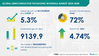
NEW YORK, June 6, 2024 /PRNewswire/ — The global semiconductor packaging materials market size is estimated to grow by USD 9.13 billion from 2024-2028, according to Technavio. The market is estimated to grow at a CAGR of over 5.3% during the forecast period. The semiconductor packaging materials market is experiencing growth due to the increasing adoption of lead-free packaging, driven by international compliance standards such as RoHS. Companies are using matte tin and nickel-palladium-silver alloys as lead substitutes in lead frame packages. Additionally, SiP packages, which can contain multiple ICs and passive components in a single package, are gaining popularity for system integration and cost benefits. Flip-chip technology, which reduces interconnect length and signal inductance, is also contributing to market growth. These trends are expected to continue during the forecast period.
Get detailed analysis on regions,market segments, customer landscape, and companies- View the snapshot of this report
Forecast period
2024-2028
Base Year
2023
Historic Data
2018 – 2022
Segment Covered
Material (Organic substrates, Lead frames, Bonding wires, Ceramic packages, and Others), End-user (Consumer electronics, Automotive, Medical devices, Communication and telecom, and Others), and Geography (APAC, North America, Europe, South America, and Middle East and Africa)
Region Covered
APAC, North America, Europe, South America, and Middle East and Africa
Key companies profiled
Amkor Technology Inc., ASE Technology Holding Co. Ltd., BASF SE, ChipMOS TECHNOLOGIES INC., DuPont de Nemours Inc., Henkel AG and Co. KGaA, Heraeus Holding GmbH, Hitachi Ltd., Honeywell International Inc., Indium Corp., Intel Corp., KYOCERA Corp., LG Innotek Co. Ltd., MITSUI and CO. LTD., Nan Ya Printed Circuit Board Corp., Nippon Steel Corp., Powertech Technology Inc., Samsung Electronics Co. Ltd., Taiwan SEMICONDUCTOR CO. LTD., and Texas Instruments Inc.
Key Market Trends Fueling Growth
The Semiconductor Packaging Materials market is experiencing significant growth due to the increasing demand for advanced electronic devices. Dielectrics, substrates, and encapsulants are key packaging materials used in this industry. Notable trends include the use of advanced materials like organics and polymers for substrates, and the adoption of chip-on-film and flip chip packaging technologies.
Leadframe materials, such as copper and lead, are also in high demand. Solder materials play a crucial role in the assembly process, while adhesives ensure the reliability and durability of the packages. The market is expected to continue its upward trajectory, driven by the need for smaller, faster, and more energy-efficient devices.
Market Challenges
The semiconductor packaging materials market faces challenges due to the increasing cost of manufacturing ICs. With the demand for compact ICs and new 3D packaging solutions, fabrication plants require expensive equipment. The complex manufacturing process and higher probability of defects add to the overall cost.Rapid technology advances in the semiconductor industry further increase equipment costs. As a result, companies are outsourcing fabrication to specialized foundries, reducing potential customers for packaging materials vendors. This trend could impact the market’s growth during the forecast period.The semiconductor packaging materials market faces several challenges in delivering advanced solutions. Dielectrics, such as silicon oxide and silicon nitride, are crucial for insulation and protection. However, their high cost and limited thermal stability pose challenges. Ceramics and composites are alternatives, offering better thermal properties but with challenges in uniformity and consistency. Soldering materials, like solder pastes and preforms, ensure reliable electrical connections.Yet, the need for high-temperature and low-melting-point materials creates challenges. Adhesives, like epoxies and silicones, bond various components together. However, ensuring compatibility with different materials and maintaining reliability over time remains a challenge. Overall, the semiconductor packaging materials market requires continuous innovation to address these challenges and deliver high-performance, cost-effective, and reliable solutions.
Research report provides comprehensive data on impact of trend, driver and challenges – Download a Sample Report
Segment Overview
Material 1.1 Organic substrates1.2 Lead frames1.3 Bonding wires1.4 Ceramic packages1.5 OthersEnd-user 2.1 Consumer electronics2.2 Automotive2.3 Medical devices2.4 Communication and telecom2.5 OthersGeography 3.1 APAC3.2 North America3.3 Europe3.4 South America3.5 Middle East and Africa
1.1 Organic substrates- The organic substrates market for semiconductor packaging materials is projected to expand significantly during the forecast period. These materials serve as the foundation for individual semiconductor devices and ICs, requiring them to be efficient conductors of electricity and thin for use in demanding applications. Organic substrates, surrounded by low-loss and ultra-thin dielectric materials, are increasingly preferred over lead frames and bonding wires due to their flexibility as interconnects.
Samsung Electro-Mechanics is a key vendor offering advanced organic substrates for various industries, including mobile devices, automotive, and IoT, featuring build-up layers and high-density interconnections. The increasing demand for semiconductor packaging will fuel the growth of the organic substrates segment in the global semiconductor packaging materials market.
For more information on market segmentation with geographical analysis including forecast (2024-2028) and historic data (2018 – 2022) – Download a Sample Report
Research Analysis
The Semiconductor Packaging Materials Market encompasses various components essential for the production of semiconductor packages. These materials include Packaging Technologies, such as Liquid Encapsulation and Wafer Bonding. Leadframes and Substrates, like IC Substrates and Tape Substrates, serve as the foundation for semiconductor devices. Encapsulation Resins and Die Attach Materials ensure the protection and attachment of semiconductor dies. Underfill Materials enhance the reliability and durability of semiconductor packages.
Bonding Wires and Solder Balls facilitate the interconnection of semiconductor components. Photopolymer Films and Electroless Plating contribute to the production process through their role in photolithography and electroless deposition, respectively. Dielectric Materials provide insulation and electrical separation within semiconductor packages. Through-Silicon Vias enable the vertical interconnection of semiconductor layers. Collectively, these materials play a crucial role in the semiconductor industry, driving innovation and advancements in technology.
Market Research Overview
The Semiconductor Packaging Materials market encompasses various components used in the production and protection of semiconductor devices. These materials include adhesives, encapsulants, underfills, substrates, and solder materials. Adhesives are used to attach components to the substrate, while encapsulants provide protection to the semiconductor die.
Underfills fill the gaps between the die and the substrate, ensuring proper electrical connection. Substrates serve as the base for the semiconductor components, while solder materials are used to connect the semiconductor die to the package pins. The use of these materials is essential in the semiconductor industry to ensure the functionality and reliability of electronic devices.
Table of Contents:
1 Executive Summary
2 Market Landscape
3 Market Sizing
4 Historic Market Size
5 Five Forces Analysis
6 Market Segmentation
MaterialOrganic SubstratesLead FramesBonding WiresCeramic PackagesOthersEnd-userConsumer ElectronicsAutomotiveMedical DevicesCommunication And TelecomOthersGeographyAPACNorth AmericaEuropeSouth AmericaMiddle East And Africa
7 Customer Landscape
8 Geographic Landscape
9 Drivers, Challenges, and Trends
10 Company Landscape
11 Company Analysis
12 Appendix
About Technavio
Technavio is a leading global technology research and advisory company. Their research and analysis focuses on emerging market trends and provides actionable insights to help businesses identify market opportunities and develop effective strategies to optimize their market positions.
With over 500 specialized analysts, Technavio’s report library consists of more than 17,000 reports and counting, covering 800 technologies, spanning across 50 countries. Their client base consists of enterprises of all sizes, including more than 100 Fortune 500 companies. This growing client base relies on Technavio’s comprehensive coverage, extensive research, and actionable market insights to identify opportunities in existing and potential markets and assess their competitive positions within changing market scenarios.
Contacts
Technavio Research
Jesse Maida
Media & Marketing Executive
US: +1 844 364 1100
UK: +44 203 893 3200
Email: media@technavio.com
Website: www.technavio.com/
View original content to download multimedia:https://www.prnewswire.com/news-releases/semiconductor-packaging-materials-market-size-is-set-to-grow-by-usd-9-13-billion-from-2024-2028–increasing-miniaturization-of-electronic-devices-and-growing-application-of-semiconductor-ics-in-iot-to-boost-the-market-growth-tech-302164850.html
SOURCE Technavio


 Coin Market5 days ago
 Technology5 days ago
 Coin Market5 days ago
 Technology4 days ago
 Technology4 days ago
 Technology5 days ago
 Coin Market5 days ago
 Technology5 days ago